
Calculate first-pass rectangular microstrip patch width and length from center frequency, substrate Dk, and patch-to-ground dielectric height.
Table of contents
How to use our Microstrip Patch Antenna Dimensions Calculator
- Enter the center frequency from the RF requirement, then choose the matching GHz or MHz unit.
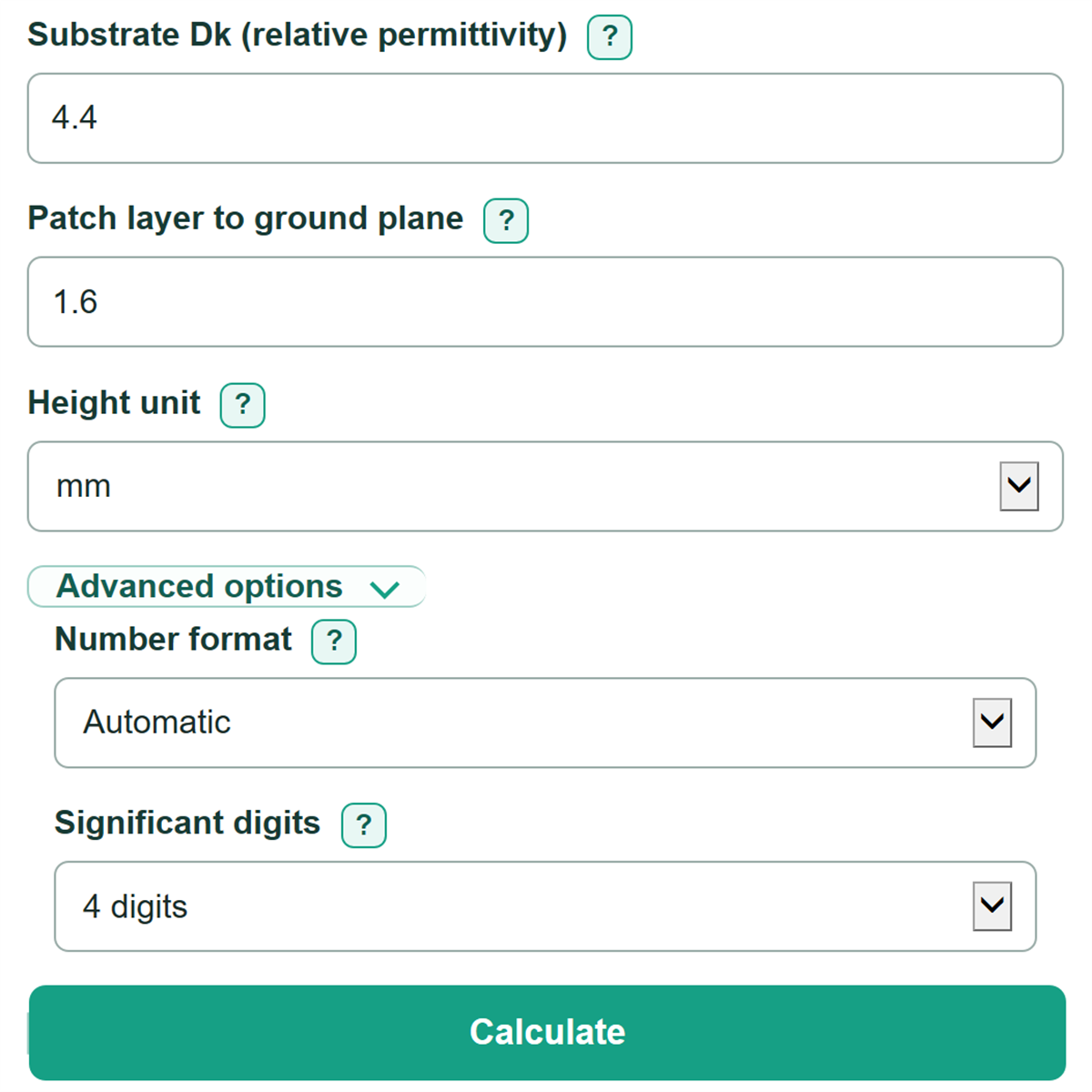
- Enter the substrate Dk for the exact laminate and the dielectric height from the patch copper to its adjacent ground plane. Choose the height unit shown in the PCB stackup.
- Open Advanced options only if you want to change the displayed number format or significant digits, then select Calculate.
- Check that the effective Dk is between 1 and the entered substrate Dk when the entered Dk is above 1. Also confirm that the mm, mil, and inch results are equivalent dimensions before copying them into CAD.
Definitions
Substrate Dk (relative permittivity): A dimensionless material value that describes how the substrate changes electric fields and wave speed compared with vacuum.
Patch layer to ground plane: The dielectric spacing from the patch copper to its adjacent reference ground plane. It is not always the total finished PCB thickness.
Effective Dk: The model's estimated permittivity after accounting for fields traveling partly through the substrate and partly through air.
Edge fringe extension: The extra electrical length at each radiating edge caused by fields extending beyond the metal patch.
TM10: The basic rectangular patch resonance used by this method, with patch length as the main resonant direction.
Mil: One thousandth of an inch, so 1 inch equals 1,000 mil.
Common mistakes and quick fixes
Mistake: Entering 2450 while the frequency unit is set to GHz.
Fix: Select MHz for 2450, or enter 2.45 with GHz selected.
Mistake: Using total board thickness as the patch-to-ground height on a multilayer PCB.
Fix: Copy only the dielectric spacing from the patch copper to its adjacent reference ground plane.
Mistake: Assuming 4.4 is the correct Dk for every material described as FR4.
Fix: Use the Dk for the exact laminate, construction, frequency, and test condition listed by the fabricator or material data sheet.
Mistake: Selecting a height unit that does not match the stackup value or typed unit suffix.
Fix: Select mm, mil, or inch exactly as shown in the stackup. The calculator converts the current value when you change units.
Mistake: Treating extra significant digits as extra physical accuracy.
Fix: Use significant digits only to control displayed rounding. Material data and fabrication tolerances limit real accuracy.
Mistake: Treating the calculated patch length as a guaranteed fabricated resonant length.
Fix: Use it as a starting dimension for EM simulation, fabrication review, measurement, and tuning.
Limitations & Key Assumptions / Boundary Conditions
- The equations produce a first-pass rectangular TM10 patch geometry, not a guaranteed fabricated resonance.
- Center frequency and patch-to-ground height must be greater than zero, and substrate Dk must be at least 1.
- The model treats the substrate as uniform and uses one entered Dk. Actual laminate Dk can vary with construction, frequency, and test method.
- The model does not include finite ground-plane size, feed loading, copper thickness, conductor or dielectric loss, solder mask, enclosures, nearby parts, or full-wave coupling.
- The calculator does not determine feed position, input impedance, bandwidth, gain, radiation efficiency, or matching-network values.
- Material variation and fabrication tolerances can shift resonance, so final dimensions normally require EM simulation and measured tuning.
- A large dielectric height can make the calculated physical length zero or negative. The calculator rejects that geometry instead of showing it as usable.
- Number format and significant digits change displayed rounding only. They do not improve model or fabrication accuracy.
Methodology
Calculation method
The calculator converts center frequency to hertz and patch-to-ground dielectric height to meters. Changing a unit selector converts the current number so the same physical frequency or height is preserved. It then uses the rectangular microstrip transmission-line method to calculate patch width, effective Dk, edge fringe extension, effective resonant length, and physical patch length [1].
In the formulas, W is patch width, L is physical patch length, Leff is effective resonant length, h is dielectric height, f is center frequency, and c is the speed of light. The term εr is substrate Dk, εeff is effective Dk, and ΔL is fringe extension at one radiating edge. The function sqrt means square root.
W = c / (2 * f) * sqrt(2 / (εr + 1))
W/h = patch width / dielectric height
εeff = (εr + 1) / 2 + (εr - 1) / 2 * (1 + 12 / (W/h))^(-1/2)
ΔL = 0.412 * h * [((εeff + 0.3) * (W/h + 0.264)) / ((εeff - 0.258) * (W/h + 0.8))]
Leff = c / (2 * f * sqrt(εeff))
L = Leff - 2 * ΔL
The calculation uses the exact vacuum speed of light, c = 299,792,458 m/s [2]. It keeps unrounded meter values through the calculations, then converts the finished geometry using 1 inch = 25.4 mm and 1 inch = 1,000 mil [3]. Number format and significant digits are applied only when results are displayed.
Worked example
For 2.45 GHz, a substrate Dk of 4.4, and a patch-to-ground height of 1.6 mm, the model gives a patch width of about 37.23 mm and an effective Dk of 4.081. The estimated fringe extension is 0.7386 mm at each radiating edge, giving a physical patch length of about 28.81 mm. The same patch is about 1,466 mil by 1,134 mil, or 1.466 inches by 1.134 inches.