
Estimate MOSFET heat, optional gate-drive power, and junction temperature from current, RDS(on), switching data, and thermal resistance.
Table of contents
How to use our MOSFET Power Dissipation Calculator
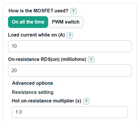
- Choose How is the MOSFET used? Pick On all the time for a DC load switch, or PWM switch when the MOSFET turns on and off repeatedly.
- Enter Load current while on, On-resistance RDS(on), and any PWM fields that are visible: On time, Voltage during switching, Switching rate, and Rise plus fall time.
- Open Advanced options only when you have extra datasheet or board data, such as Hot on-resistance multiplier, Output capacitance Coss, Total gate charge Qg, or Thermal resistance junction-to-air.
- Click Calculate, then read Estimated MOSFET heat first. Use Thermal check and Estimated junction temperature only if you entered thermal data.
- Sanity-check the loss split: high current should raise On-resistance loss, while higher Switching rate, Voltage during switching, or Rise plus fall time should raise Turn-on and turn-off loss.
Definitions
RDS(on): The drain-to-source resistance of the MOSFET when it is fully turned on. Lower RDS(on) usually means less heat at the same current.
On time: In PWM mode, the percent of each switching cycle when the MOSFET is on.
Rise plus fall time: The total transition time used for the simple switching loss estimate. Longer transitions usually make more heat.
Coss: Output capacitance from the MOSFET drain-to-source region. Charging and discharging it can add switching loss.
Qg: Total gate charge. It estimates gate-drive power, which is shown separately from MOSFET drain heat.
Thermal resistance junction-to-air: The temperature rise from the MOSFET chip to nearby air per watt of heat, in deg C/W.
Temperature margin: Max junction temperature minus Estimated junction temperature. A negative value means the estimate is over the entered limit.
Common mistakes and quick fixes
Mistake: Entering the full load current for Load current while on when only part of the current flows through this MOSFET.
Fix: Use the current through this one MOSFET while it is on, not the total system current.
Mistake: Using a room-temperature On-resistance RDS(on) without adjusting for heating.
Fix: Enter the datasheet hot value, or use Hot on-resistance multiplier to raise the resistance.
Mistake: Mixing up On time with off time in PWM switch mode.
Fix: Enter the percent of each cycle that this MOSFET is on in On time.
Mistake: Counting Gate-drive power as part of Estimated MOSFET heat.
Fix: Keep Gate-drive power separate unless your specific layout makes that driver loss heat the MOSFET package.
Mistake: Entering Thermal resistance junction-to-air from a datasheet test board and expecting the same board temperature.
Fix: Use a value that matches your copper area, airflow, and package, or treat Thermal check as a first estimate.
Limitations & Key Assumptions / Boundary Conditions
- This is a first-order estimate for a hard-switched MOSFET. It does not replace a datasheet safe-operating-area check, lab temperature test, or circuit simulation.
- DC mode ignores On time, Voltage during switching, Switching rate, Rise plus fall time, Coss, and Qg. Hidden PWM fields do not affect the DC result.
- Turn-on and turn-off loss uses a triangle overlap estimate. Real waveforms, gate resistance, driver strength, Miller plateau behavior, and layout parasitics can change the result.
- Output-capacitance loss uses the entered Coss as a fixed value. Real Coss changes with voltage, so the estimate can be high or low.
- Gate-drive power is shown separately and is not added to Estimated MOSFET heat. In some packages or layouts, part of that energy may still heat nearby parts.
- Thermal resistance junction-to-air depends strongly on copper area, airflow, package mounting, and nearby hot parts. A pass result still needs a real temperature check.
- The calculator does not include avalanche energy, reverse recovery, body-diode dead-time loss, pulsed transient thermal impedance, current sharing, or switching-node ringing.
Methodology
Calculation steps
The calculator first converts the entered On-resistance RDS(on) from milliohms to ohms and applies the Hot on-resistance multiplier.
R_hot_ohm = (rds_on_mohm / 1000) * rds_temp_factor
It then sets the on-time fraction. DC mode uses a full on-time fraction of 1. PWM mode uses the entered On time percent.
D = 1 for dc mode; D = duty_percent / 100 for pwm mode
On-resistance loss is current squared times hot resistance times the on-time fraction.
P_cond = load_current_a^2 * R_hot_ohm * D
In PWM mode, turn-on and turn-off loss uses a simple voltage-current overlap estimate with a 0.5 factor for the triangular transition shape [1].
P_sw = 0.5 * switch_voltage_v * load_current_a * (rise_fall_ns * 1e-9) * (switch_freq_khz * 1000)
If Output capacitance Coss is entered, the calculator adds output-capacitance switching loss using energy equals one-half capacitance times voltage squared, repeated at the switching rate [3].
P_coss = 0.5 * (coss_pf * 1e-12) * switch_voltage_v^2 * (switch_freq_khz * 1000)
If Total gate charge Qg is entered, the calculator estimates gate-drive power, but it does not add that value to MOSFET heat.
P_gate = (gate_charge_nc * 1e-9) * gate_drive_v * (switch_freq_khz * 1000)
The main heat result is the sum of drain-path heat terms only.
P_heat = P_cond + P_sw + P_coss
When Thermal resistance junction-to-air is entered, estimated junction temperature is nearby air temperature plus heat times thermal resistance. Temperature margin is the entered maximum junction temperature minus that estimate.
T_j = ambient_temp_c + P_heat * theta_ja_c_per_w
margin = max_junction_temp_c - T_j
Mini-example
For a PWM switch with 8 A load current, 15 milliohms RDS(on), 1.2 hot multiplier, 40% on time, 48 V switching voltage, 100 kHz switching rate, 60 ns rise plus fall time, 500 pF Coss, and 30 deg C/W thermal resistance at 40 deg C air, the calculator gets 0.4608 W on-resistance loss, 1.152 W turn-on and turn-off loss, 0.0576 W output-capacitance loss, and 1.6704 W Estimated MOSFET heat. The estimated junction temperature is 90.112 deg C, so the margin to a 150 deg C limit is 59.888 deg C.
Important calculation choices
All numeric parsing uses the units shown in the labels: milliohms, kHz, ns, nC, pF, volts, amps, watts, and deg C. Optional fields are only included when entered. Gate-drive power is separated because it is usually handled by the driver path, while Thermal check uses Estimated MOSFET heat.