
Enter your current, allowed copper heating, thickness, and layer to estimate the preliminary PCB trace width needed in mil and mm.
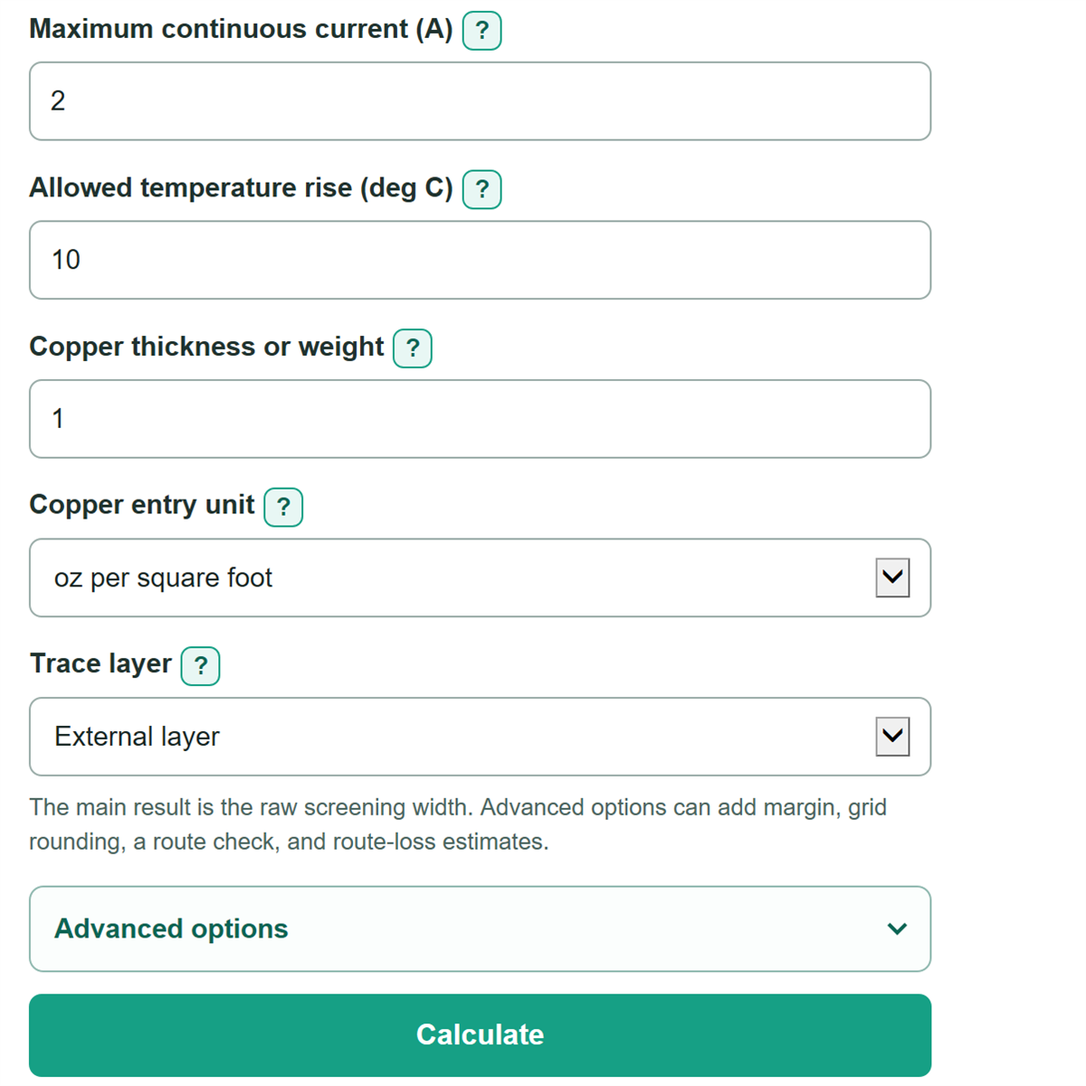
The main result is the raw screening width. Advanced options can add margin, grid rounding, a route check, and route-loss estimates.
Advanced options
Routing target
Planned route check
Route loss estimate
Calculation details
Table of contents
How to use our PCB Trace Width Calculator
- Enter the highest continuous current expected on the copper path. Use sustained current, not a brief startup or surge peak.
- Enter the allowed temperature rise, which is how many degrees C warmer the trace may get than its surroundings.
- Enter the copper value from the stackup or fabricator and choose the matching unit, then select whether the trace is on an external or internal layer.
- Select Calculate and use the preliminary minimum width as an early layout estimate. In Advanced options, add a margin and routing grid to create a rounded-up width target.
- If the route is drawn, enter its narrowest finished width and compare it with the target. A pass only checks this trace-width screen, so also review voltage drop, vias, pads, connectors, and thermal conditions.
Definitions
Continuous current: The highest current that flows for a sustained time in the trace, measured in amperes (A).
Allowed temperature rise: The amount the copper may warm above the surrounding board environment, measured in degrees C.
External layer: A copper layer on the outside surface of a PCB.
Internal layer: A copper layer buried between other PCB layers.
mil: One thousandth of an inch. One mil equals 0.0254 mm.
Copper cross-section: The copper area seen in a cut across the trace. It is trace width times copper thickness and is measured here in mil^2.
Fab-ready width target: The raw minimum width after the selected extra margin and upward rounding to the selected grid.
Voltage drop: Voltage lost along a copper path because the path has electrical resistance.
Common mistakes and quick fixes
Mistake: Entering ambient temperature as the allowed temperature rise.
Fix: Enter only the permitted increase above ambient, such as 10 degrees C.
Mistake: Treating nominal 1 oz copper as the finished thickness of an external trace.
Fix: Enter the finished thickness from the fabricator when available, especially where external plating changes the copper thickness.
Mistake: Selecting an external layer for copper buried inside the board.
Fix: Choose Internal layer for a trace between board layers. It uses a different conductor-sizing coefficient.
Mistake: Checking the average track width instead of the narrowest part of the route.
Fix: Enter the smallest current-carrying neck-down or pad entry as the narrowest finished trace width.
Mistake: Routing at the raw calculated minimum width.
Fix: Add the margin required by the project, then round upward to the layout or fabrication grid.
Mistake: Treating a passing width check as approval for the whole power path.
Fix: Check vias, thermal-relief spokes, connectors, copper planes, local heat sources, and voltage-drop limits separately.
Limitations & Key Assumptions / Boundary Conditions
- This is a preliminary continuous-current estimate using the historical IPC-2221 conductor-sizing curve fit; it is not a complete thermal simulation, controlled-impedance calculation, or production approval.
- The calculation assumes a copper conductor and separate external or internal layer coefficients. Stackup, nearby copper, planes, airflow, enclosure temperature, and local heat sources can change actual trace temperature.
- Optional resistance is estimated at 20 degrees C. Actual resistance changes with copper temperature, plating, etching, pads, vias, connectors, and other series elements.
- The route check applies only to the entered narrowest finished trace segment. A wider section elsewhere does not offset a narrow neck-down.
- Short pulses, surge current, fusing behavior, vias, connectors, thermal-relief spokes, parallel paths, and return-path design are outside this calculation.
- The calculator converts nominal 1 oz per square foot copper to 1.37 mil. Use direct finished thickness when the fabricator provides it.
Methodology
Width calculation
The calculator uses the historical IPC-2221 empirical curve fit as an early copper-conductor sizing screen. It calculates required copper cross-section from continuous current, allowed temperature rise, and the selected trace location. The external-layer coefficient is 0.048, and the internal-layer coefficient is 0.024.
A = (I / (k x ΔT^0.44))^(1 / 0.725)
A is required copper cross-section in mil^2, I is continuous current in A, k is the coefficient for the selected layer, and ΔT is allowed temperature rise in degrees C.
W = A / t
W is minimum trace width in mil, and t is copper thickness in mil. The calculator also converts width using 1 mil = 0.0254 mm.
Margin and route check
The optional margin increases the raw width before grid rounding. When a positive grid is entered, the target rounds upward to a whole grid increment. An entered narrowest width passes this numerical check only when it is at least the rounded target.
W_margin = W x (1 + margin / 100)
W_target = ceil(W_margin / grid) x grid
Optional route loss
When path length is entered, resistance is calculated with the fab-ready width unless a narrowest finished width was entered. The estimate uses copper resistivity at 20 degrees C of 1.724 x 10^-8 ohm m, then calculates voltage drop and copper power loss.
R = ρL / (W x t)
V_drop = I x R; P_loss = I^2 x R
Worked mini-example
For 2 A, a 10 degrees C allowed rise, 1 oz per square foot copper, and an external layer, the raw estimate is about 31.0 mil. A 20% margin makes it about 37.2 mil, and a 1 mil grid rounds the routing target up to 38 mil.