
Enter your PCB stackup to estimate single-ended trace impedance or calculate a starting trace width for a target impedance.
Stackup values
Table of contents
How to use our PCB Trace Impedance Calculator
- Select "Trace impedance" when you know the routed width, or select "Trace width for a target" when you know the required single-ended impedance.
- Choose "Outer-layer microstrip" for a trace above one reference plane, or "Symmetric inner-layer stripline" for a centered inner trace between two equally spaced reference planes.
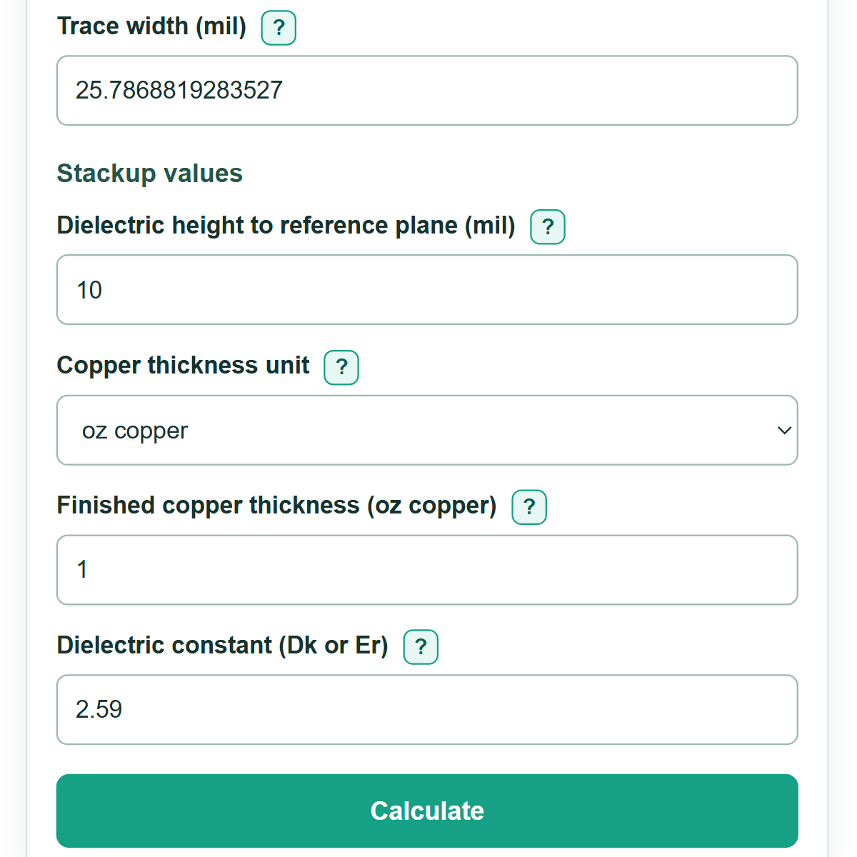
- Select the units used by the stackup, then enter dielectric height, finished copper thickness, and dielectric constant.
- Enter the visible trace width or target impedance field, then select "Calculate".
- Sanity-check the answer before using it: for the same stackup, a wider trace normally has lower impedance. Confirm a controlled-impedance width with the fabricator.
Definitions
Characteristic impedance: The single-ended impedance of a transmission line, measured in ohms.
Microstrip: An outer-layer trace with one nearby reference plane below it.
Symmetric stripline: An inner-layer trace centered between two reference planes at equal dielectric distances.
Dielectric height: The insulation distance from a trace to its reference plane. It is not the full PCB thickness.
Dielectric constant (Dk or Er): A unitless material property used to model the board insulation in the impedance equation.
Finished copper thickness: The thickness of copper on the signal layer after fabrication steps.
mil: One thousandth of an inch, equal to 0.0254 mm.
Common mistakes and quick fixes
Mistake: Entering total board thickness as dielectric height.
Fix: Enter the dielectric distance from the trace to its reference plane. For symmetric stripline, enter the equal distance from the trace to each plane.
Mistake: Using the microstrip model for an inner-layer trace.
Fix: Use "Outer-layer microstrip" only for an outer trace above one plane. Use "Symmetric inner-layer stripline" only for a centered inner trace between equally spaced planes.
Mistake: Changing from mil to mm while keeping the same number.
Fix: Select the stackup unit before entering values. If you change a unit later, the calculator converts entered dimensions to preserve their physical size.
Mistake: Treating copper weight as exact finished thickness.
Fix: Use finished copper thickness from the fabricator when available. Copper stated in oz is converted only to a nominal thickness.
Mistake: Using a generic laminate Dk for a released controlled-impedance design.
Fix: Use the construction-specific Dk in the fabricator stackup or impedance profile when possible, then request confirmation of the released routing width.
Limitations & Key Assumptions / Boundary Conditions
- This is a first-pass, single-ended planning estimate, not a fabrication guarantee.
- The microstrip model applies to an outer-layer trace above one reference plane.
- The stripline model applies only to a centered trace with equal dielectric spacing to two reference planes.
- The calculation does not include solder mask, coplanar copper, asymmetric stripline, differential pairs, glass weave, copper roughness, etched trace shape, or manufacturing tolerance.
- Dk can vary with laminate construction, resin content, test method, and frequency, so a generic datasheet value can differ from the fabricator's stackup value.
- Copper entered in oz is converted to nominal thickness. Use fabricator-supplied finished copper thickness when it is available.
Methodology
Calculation method
The calculator converts entered dimensions to mm, applies the selected closed-form single-ended model, and converts a solved width back to the selected dimension unit. Changing a unit selector converts entered dimensions so their physical size stays the same.
b = 2h + t
For symmetric stripline, b is the spacing between reference planes, h is the equal dielectric height from the trace to each plane, and t is copper thickness.
Z0 = 87 / sqrt(εr + 1.41) * ln(5.98h / (0.8w + t))
This microstrip equation uses Z0 for impedance in ohms, εr for dielectric constant, w for trace width, h for dielectric height, and t for copper thickness.
Z0 = 60 / sqrt(εr) * ln(1.9b / (0.8w + t))
This symmetric stripline equation applies only to the centered, two-plane arrangement selected in the calculator. [1]
For the width task, the calculator rearranges the selected equation to solve for w. It stops if the logarithm is not positive or if the solved width is zero or negative.
Worked example
For a microstrip with h = 10 mil, t = 1 mil, εr = 2.59, and a target of 43.5 ohms, the reversed equation gives w = 26.248988... mil. The displayed estimated width is 26.2490 mil.
Units and rounding
One mil is 0.0254 mm, one inch is 25.4 mm, and one oz copper is converted as 0.03479 mm of nominal thickness. Impedance is shown to two decimal places and solved width to four decimal places, while the calculation keeps unrounded values.