
Calculate the two crystal load capacitors and see how close common pF values get to the datasheet load capacitance.
Table of contents
How to use our Crystal Load Capacitance Calculator
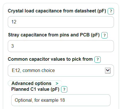
- Enter the Crystal load capacitance from datasheet in pF; this is the total load the crystal should see, not each capacitor value.
- Enter the Stray capacitance from pins and PCB in pF, then choose the Common capacitor values to pick from: E6, E12, or E24.
- Open Advanced options only if you want to check a real schematic: fill both Planned C1 value and Planned C2 value, and set Capacitor tolerance if needed.
- Click Calculate and start with Calculated value for C1 and C2, then compare it with Nearest common capacitor value and Load error with nearest common value.
- Sanity-check the output: if the load error is large or the tolerance range misses the datasheet value, consider a closer E-series list, unequal C1 and C2, or the oscillator maker's layout guidance.
Definitions
Crystal load capacitance from datasheet: The load capacitance, often marked CL, that the crystal maker expects the oscillator circuit to provide.
Stray capacitance from pins and PCB: Extra capacitance from microcontroller pins, crystal pads, traces, sockets, and nearby copper.
Planned C1 value: The capacitor value from one crystal pin to ground in your schematic.
Planned C2 value: The capacitor value from the other crystal pin to ground in your schematic.
Common capacitor values to pick from: The E6, E12, or E24 set used to round the ideal pF value to a real capacitor value.
Load error: Calculated load capacitance minus the datasheet load capacitance, in pF.
Picofarad (pF): A very small capacitance unit equal to 0.000000000001 farad.
Common mistakes and quick fixes
Mistake: Using Crystal load capacitance from datasheet as the value for each outside capacitor.
Fix: Enter it as the target total load, then use Calculated value for C1 and C2 as the ideal value for each capacitor.
Mistake: Leaving Stray capacitance from pins and PCB at 0 pF when the board and chip pins add capacitance.
Fix: Use a realistic estimate for Stray capacitance from pins and PCB, or measure/confirm it from the oscillator design notes if accuracy matters.
Mistake: Filling only Planned C1 value or only Planned C2 value.
Fix: Fill both Planned C1 value and Planned C2 value, or clear both boxes to use the nearest equal-value recommendation.
Mistake: Treating Load error with nearest common value as always positive.
Fix: Read the sign: positive means too much load, and negative means too little load compared with the datasheet value.
Mistake: Ignoring Capacitor tolerance when the pF error is small.
Fix: Set Capacitor tolerance to the part's rated percent and review Lowest likely load with tolerance and Highest likely load with tolerance.
Limitations & Key Assumptions / Boundary Conditions
- This calculator is for parallel-resonant crystals used in Pierce-style oscillator circuits. It is not for canned oscillator modules or series-resonant designs.
- Stray capacitance is an estimate unless you measure it or get it from the chip and PCB design data. A wrong stray value shifts every result.
- The nearest E-series value is a starting point. Some oscillator circuits also require checks for drive level, gain margin, ESR, startup time, and layout.
- The tolerance range assumes both capacitors move together to their low or high limit. Real parts may land anywhere inside their tolerance range.
- The calculator does not estimate frequency error in ppm because that also needs crystal pullability or motional parameters.
- Very small or unusual capacitor values may not be practical with normal PCB stray capacitance, package parasitics, and component availability.
Methodology
Core calculation
The calculator uses the standard load-capacitance relationship for two capacitors from the crystal pins to ground plus stray capacitance [2].
C_load_actual = (C1 * C2) / (C1 + C2) + C_stray
When C1 and C2 are equal, the ideal value for each outside capacitor is found by rearranging that equation.
C_equal = 2 * (C_L - C_stray)
This equal-capacitor formula is only valid when C_L is greater than C_stray. If stray capacitance is equal to or higher than the datasheet value, the ideal outside capacitor value would be zero or negative, so the calculator blocks the input.
Rounding to a real capacitor
The calculator generates candidate capacitor values from the selected E6, E12, or E24 base list over practical pF decades. It chooses the listed value with the smallest absolute difference from C_equal. If two values are equally close, it chooses the lower value.
C_load_nearest = (C_nearest / 2) + C_stray
load_error = C_load_actual - C_L
The sign is kept. A positive load error means the circuit loads the crystal more than the datasheet value. A negative load error means it loads the crystal less.
Planned parts and tolerance
If both planned capacitor values are entered, the calculator uses the full two-capacitor equation instead of assuming equal values. If planned values are not entered, the tolerance range uses the nearest common equal value for both capacitors.
C1_low = C1 * (1 - tolerance_percent / 100)
C2_low = C2 * (1 - tolerance_percent / 100)
C1_high = C1 * (1 + tolerance_percent / 100)
C2_high = C2 * (1 + tolerance_percent / 100)
low_load = (C1_low * C2_low) / (C1_low + C2_low) + C_stray
high_load = (C1_high * C2_high) / (C1_high + C2_high) + C_stray
Mini-example
For a crystal with C_L = 12 pF and C_stray = 3 pF, the ideal equal capacitor value is 2 * (12 - 3) = 18 pF. With E12 selected, the nearest common value is 18 pF. The load with 18 pF on both sides is 18 / 2 + 3 = 12 pF, so the load error is 0 pF. With 5 percent capacitor tolerance, 18 pF parts can be estimated as 17.1 pF to 18.9 pF, giving a load range from 11.55 pF to 12.45 pF.