
Estimate DC voltage drop, resistance, heat loss, and supply-voltage margin for a PCB trace using copper size and current.
Advanced options
Copper and path
Voltage budget
Table of contents
How to use our PCB Trace Voltage Drop Calculator
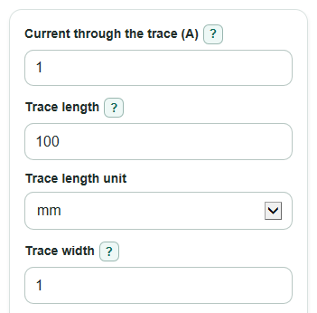
- Enter Current through the trace (A), Trace length, Trace length unit, Trace width, Trace width unit, and Copper weight (oz).
- Open Advanced options if you want to change Copper temperature (deg C), include a return path with Path to include, or split current across Identical parallel traces.
- For a budget check, enter Supply voltage for budget check (V) and Largest allowed drop (percent); leave the supply blank if you only need resistance and voltage loss.
- Select Calculate, then read Voltage lost in the copper first, followed by Voltage budget result if a supply voltage was entered.
- Sanity-check the output: a longer trace, narrower trace, hotter copper, or matching feed and return path should increase the drop; heavier copper or more Identical parallel traces should lower it.
Definitions
Current through the trace (A): The steady current flowing through the copper trace, measured in amps.
Trace length: The copper path distance from the source point to the load point.
Trace width: The finished copper width of the trace, not just the design-rule minimum.
Copper weight (oz): PCB copper thickness stated as ounces per square foot; this calculator treats 1 oz as 34.798 um thick.
Copper temperature (deg C): The estimated operating temperature of the copper, used because copper resistance changes with temperature.
Total copper resistance used: The resistance after applying copper temperature, feed/return choice, and parallel-path count.
Voltage lost in the copper: The voltage drop across the included copper path from current flowing through resistance.
Voltage budget result: A pass or fail check comparing the calculated drop with the allowed drop from your supply-voltage setting.
Current per copper area in each parallel path: Current in one parallel path divided by its copper cross-section area, shown in A/mm2.
Common mistakes and quick fixes
Mistake: Entering average current in Current through the trace (A) when the trace must carry a higher steady load.
Fix: Use the highest steady current you expect on that copper path.
Mistake: Using total board length for Trace length instead of the actual copper route from source to load.
Fix: Measure only the trace path that carries this current, and match it with Trace length unit.
Mistake: Entering design-rule minimum width in Trace width when the actual routed copper is wider or narrower.
Fix: Use the finished copper width for Trace width and the matching Trace width unit.
Mistake: Leaving Path to include on One trace only when current returns through a similar trace instead of a plane.
Fix: Choose Matching feed and return traces if the return path has about the same size and length.
Mistake: Setting Identical parallel traces to 2 or more when the paths are different lengths or not meant to share current evenly.
Fix: Use 1 unless the parallel copper paths are same-size, same-length paths with intentional current sharing.
Mistake: Reading Voltage budget result without checking Supply voltage for budget check (V) and Largest allowed drop (percent).
Fix: Enter the actual rail voltage and the voltage-drop limit from your circuit or part data sheet.
Limitations & Key Assumptions / Boundary Conditions
- This is a DC resistance estimate for simple rectangular PCB copper traces.
- It does not model AC skin effect, controlled impedance, inductance, vias, connectors, solder, copper planes, or nonuniform copper thickness.
- Copper weight is treated as uniform finished thickness, but real boards can vary after plating, etching, and fabrication tolerance.
- Identical parallel traces are assumed to share current evenly. Unequal routing can make one path carry more current.
- The matching feed and return option assumes the return trace has the same size and length as the feed trace.
- Power changed to heat in the trace is electrical loss only. It does not prove the final copper temperature is safe.
- Use a separate thermal design check or IPC-2152-style process when trace temperature rise or current capacity is the main design question.
Methodology
Core calculation
Trace resistance is based on copper resistivity, trace length, and copper cross-section area [1]. The calculator first converts your length and width to meters, converts copper weight to thickness, and then finds resistance for one trace.
t_m = copper_oz * 34.798e-6
L_m = length * length_factor
W_m = width * width_factor
area_m2 = W_m * t_m
R20_single = rho20 * L_m / area_m2
The constants used are rho20 = 1.724e-8 ohm m for copper at 20 deg C, alpha_cu = 0.00393 per deg C, and 1 oz copper thickness = 34.798 um. Unit factors are mm = 0.001 m, inch = 0.0254 m, and mil = 0.0000254 m.
Temperature, return path, and parallel traces
The copper temperature setting adjusts the one-trace resistance with a simple linear temperature factor.
R_single = R20_single * (1 + alpha_cu * (copper_temp_c - 20))
The path setting then multiplies resistance by 1 for One trace only or by 2 for Matching feed and return traces. Identical parallel traces divide the total resistance by the number of equal paths.
R_total = R_single * path_multiplier / parallel_paths
Voltage, power, and budget outputs
Voltage lost in the copper uses Ohm's law. Power changed to heat in the trace uses current squared times resistance.
V_drop = current_a * R_total
P_loss = current_a * current_a * R_total
If Supply voltage for budget check (V) is entered, the calculator also compares the drop with Largest allowed drop (percent).
drop_percent = 100 * V_drop / supply_voltage_v
voltage_at_load_v = supply_voltage_v - V_drop
budget_margin_v = supply_voltage_v * max_drop_percent / 100 - V_drop
Current density is a supporting value for each parallel path.
current_density = (current_a / parallel_paths) / area_mm2
Mini example
For 1 A through a 100 mm long, 1 mm wide, 1 oz copper trace at 20 deg C with One trace only and 1 parallel path, the calculator gets R_total = 0.04954 ohm. The voltage drop is 1 A * 0.04954 ohm = 0.04954 V, and the power loss is 1 A * 1 A * 0.04954 ohm = 0.04954 W.